Aperçu Produitsp type silicon substrate fabricant en ligne
Certificat
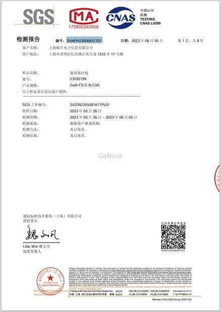
LA CHINE Shanghai GaNova Electronic Information Co., Ltd. certifications
Je suis en ligne une discussion en ligne

p type silicon substrate fabrication en ligne

(0)
Related Product
acheter JDCD10-001-005 2 pouces GaAs ((111) Substrats dopés au Zn en ligne fabricant

JDCD10-001-005 2 pouces GaAs ((111) Substrats dopés au Zn

2inch GaAs(111) Zn-doped substrates Overview GaAs crystals can be created through three different methods. One of the more common methods is the vertical gradient freeze process, which involves growing crystals and slicing them, followed by edge rounding and polishing them into wafers. Another ... Lire la suite
acheter JDCD10-001-004 2 pouces GaAs (111) Si Substrats dopés en ligne fabricant

JDCD10-001-004 2 pouces GaAs (111) Si Substrats dopés

2inch GaAs (111) Si-doped substrates Overview Gallium in a GaAs Wafer is in general used in the production of semiconductors, barometers, light emitting diodes, thermometers and electronic circuits. It is a silvery metal and quite soft which makes it easy to be used in chips as well. Gallium element... Lire la suite
acheter JDCD10-001-003 2 pouces GaAs ((100) Substrats dopés au Zn en ligne fabricant

JDCD10-001-003 2 pouces GaAs ((100) Substrats dopés au Zn

2inch GaAs(100) Zn-doped substrates Overview Gallium arsenide of a GaAs Wafer has the attribute of generating laser light from electricity in a direct manner. There are two types of GaAs Wafer; polycrystalline and single crystal. These wafers are utilized in micro electronics and opto electronics ... Lire la suite
acheter JDCD10-001-002 Substrats dopés au Si (100) GaAs de 2 pouces en ligne fabricant

JDCD10-001-002 Substrats dopés au Si (100) GaAs de 2 pouces

2inch GaAs (100) Si-doped substrates Overview GaAs is often used as a substrate material for the epitaxial growth of other III-V semiconductors, including indium gallium arsenide, aluminum gallium arsenide and others. Gallium arsenide of a GaAs Wafer has the attribute of generating laser light from ... Lire la suite
acheter JDCD04-001-007 10x10mm2(010)Sn-Doped Free-Standing Ga2O3 Monocristal Substrat Product Grade Single Polishing en ligne fabricant

JDCD04-001-007 10x10mm2(010)Sn-Doped Free-Standing Ga2O3 Monocristal Substrat Product Grade Single Polishing

10x10mm2(010)Sn-doped free-standing Ga2O3 single crystal substrate Product grade single polishing Thickness 0.6~0.8mm FWHM<350arcsec,Ra≤0.5nm Resistance 1.53E+18Ω/cm-3 Optoelectronic devices, insulating layers of semiconductor materials, and UV filters While silicon-based devices have been able to ... Lire la suite
acheter JDCD04-001-003 10x10mm2 100 ((Off 6°) Fe dopé en position libre Ga2O3 Substrate monocristallin Qualité du produit Polissage unique en ligne fabricant

JDCD04-001-003 10x10mm2 100 ((Off 6°) Fe dopé en position libre Ga2O3 Substrate monocristallin Qualité du produit Polissage unique

10x10mm2 100(off 6°) Fe-doped free-standing Ga2O3 single crystal substrate Product grade single polishing Thickness 0.6~0.8mm FWHM<350arcsec,Ra≤5nm Optoelectronic devices, insulating layers of semiconductor materials, and UV filters Power density is greatly improved in gallium nitride devices ... Lire la suite
acheter JDCD04-001-002 10x10mm2 (- 201) Sn-a enduit le polonais simple simple libre de Ga2O3 Crystal Substrate Product Grade en ligne fabricant

JDCD04-001-002 10x10mm2 (- 201) Sn-a enduit le polonais simple simple libre de Ga2O3 Crystal Substrate Product Grade

10x10mm2 (-201) Sn-doped free-standing Ga2O3 single crystal substrate Product grade single polishing Thickness 0.6~0.8mm FWHM<350arcsec,Ra≤0.3 nm Resistance Lire la suite
acheter JDCD06-001-007 Wafer de silicium de 12 pouces Dispositifs MEMS Circuits intégrés Substrats dédiés pour les dispositifs discrets en ligne fabricant

JDCD06-001-007 Wafer de silicium de 12 pouces Dispositifs MEMS Circuits intégrés Substrats dédiés pour les dispositifs discrets

12-inch silicon wafer MEMS devices, integrated circuits,dedicated substrates for discrete devices Overview A silicon wafer is a material essential for manufacturing semiconductors, which are found in all kinds of electronic devices that enrich our lives. Few of us have a chance to encounter an ... Lire la suite